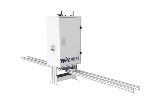
LEP-SJ68BPP-CV3R
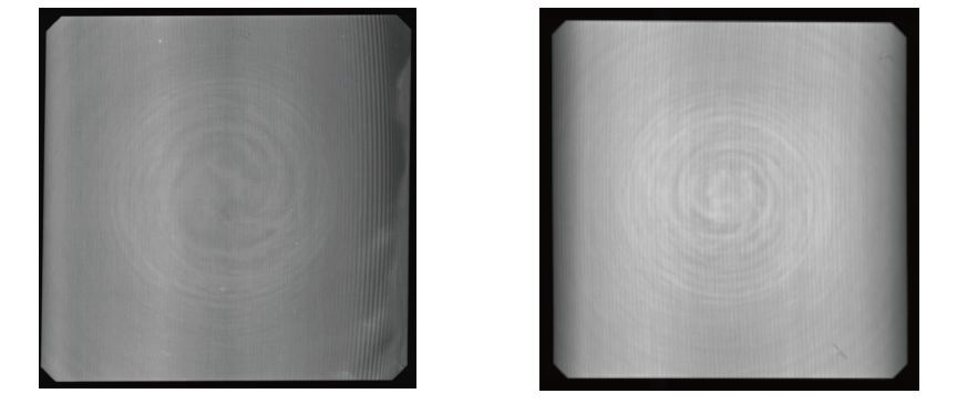
The LEP (Low Efficiency Photoluminescence) are integrated PL imaging components specially developed for the low excitation efficiency of raw silicon wafers. They can transmit the PL images of raw silicon wafers to the PC through a gigabit network. Users can use image recognition related technologies to judge and identify defects in the imaging, and cooperate with automation to eliminate them.Typical types of defects that can be detected are: hidden crack, broken edge, black center,concentric circle, scratch, belt mark and dirty.
LEP can help users eliminate defective chips in the front-end of the process to increase the production of A-grade chips, and also provide timely feedback and warning of defects in the process; It can help users identify potential product defects during the loading of raw silicon wafers, so as to make timely adjustments on site and reduce the potential waste of raw material costs in the future. In the context of increasingly large and thin silicon wafers, traditional contact detection is difficult to effectively control the fragmentation rate. However, non-destructive testing of laser PL will become an essential detection method and a standard product for removing defective products in the photovoltaic process.