EN

中文 EN

Home>Industry

Solution

The hidden crack broken edge of raw silicon wafers inspection Raw Silicon Wafers PL Inspection Post-PE Photoluminescence Inspection

Industry Pain Points

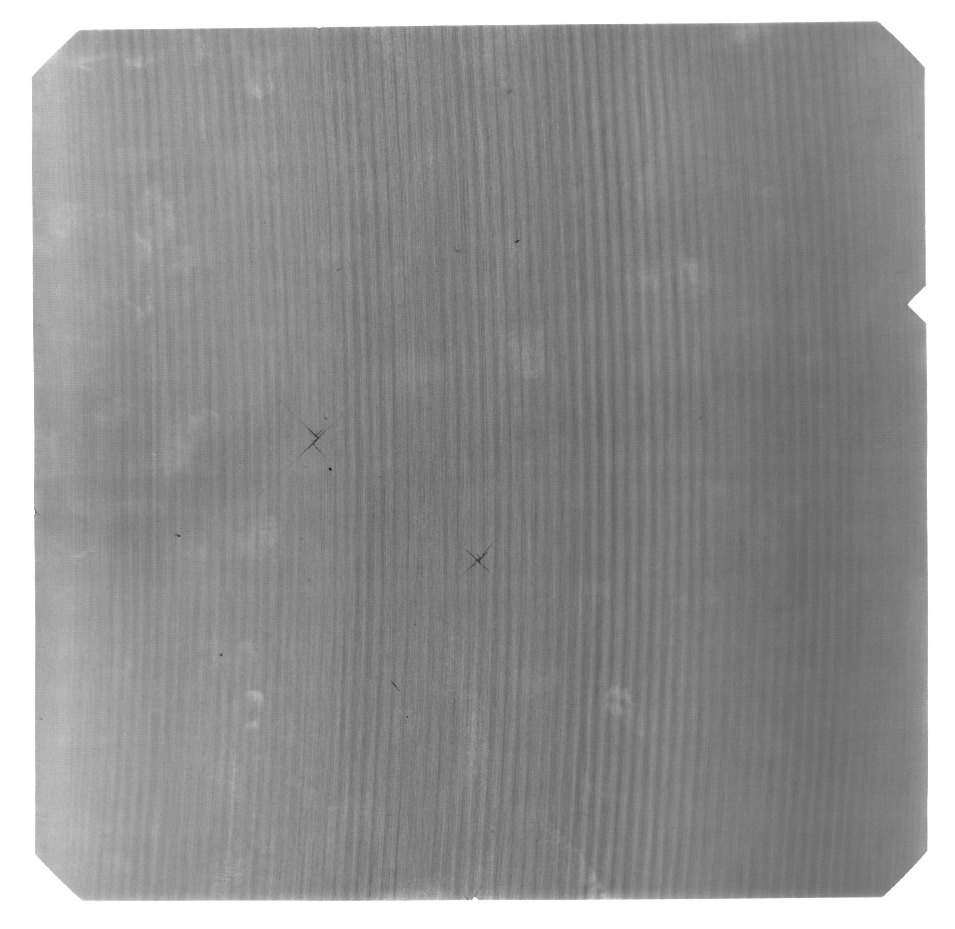
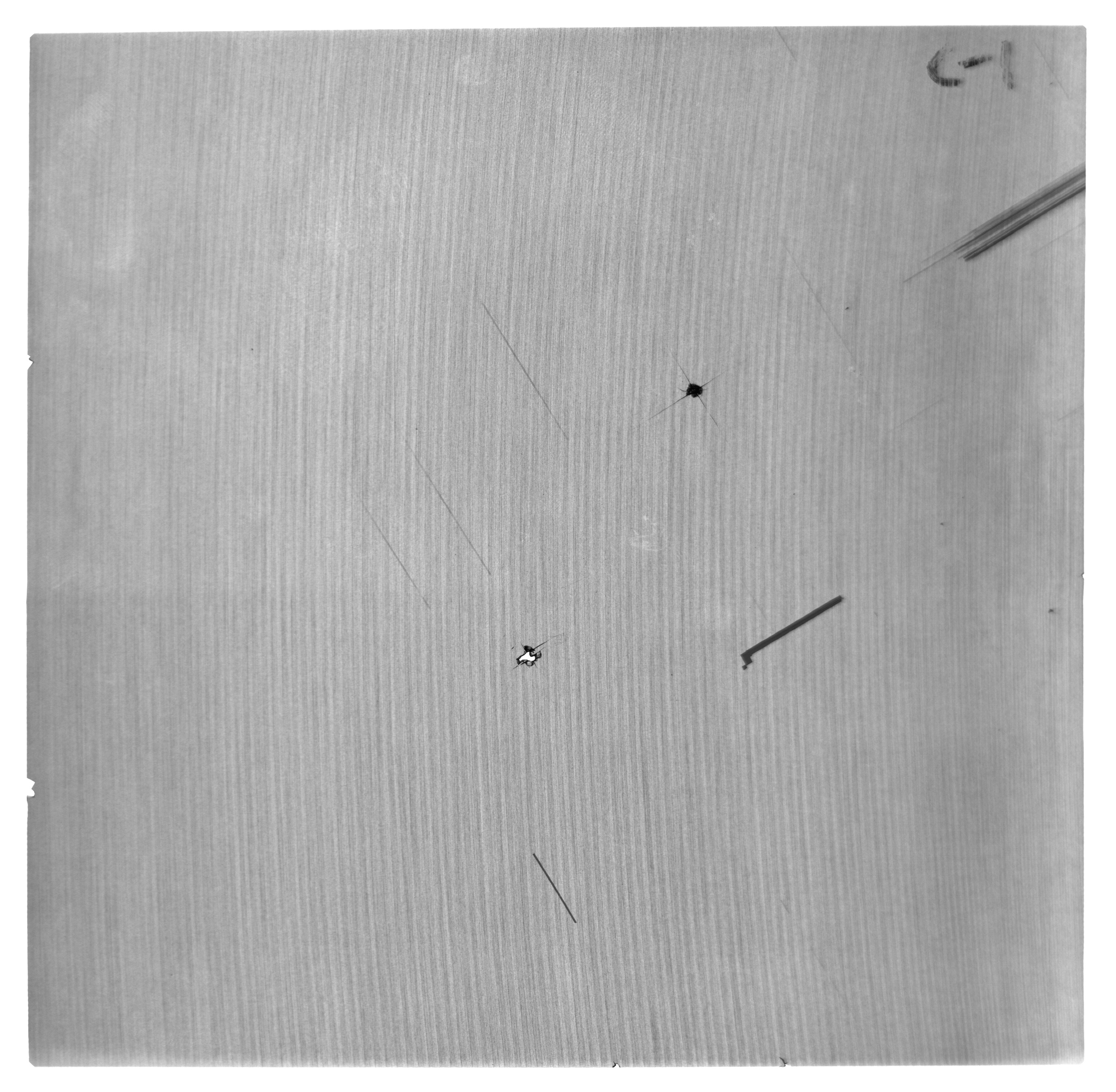
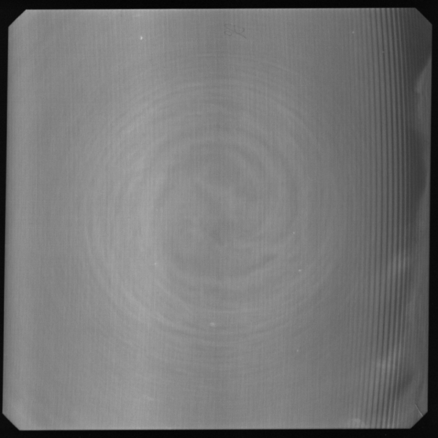
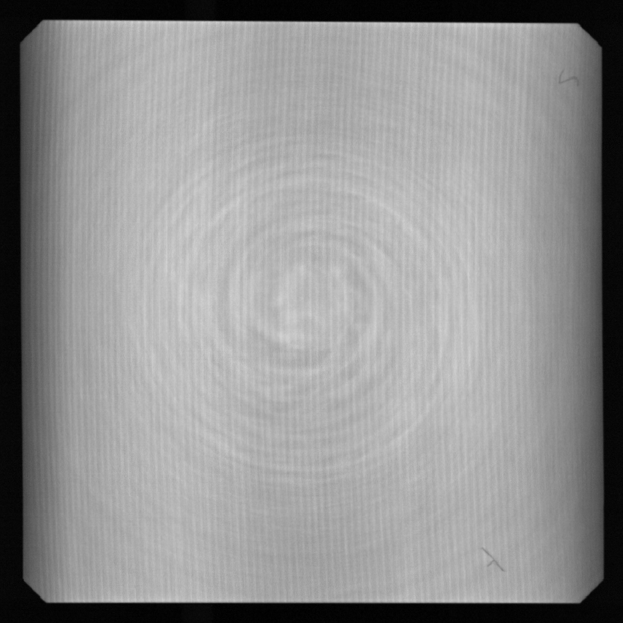
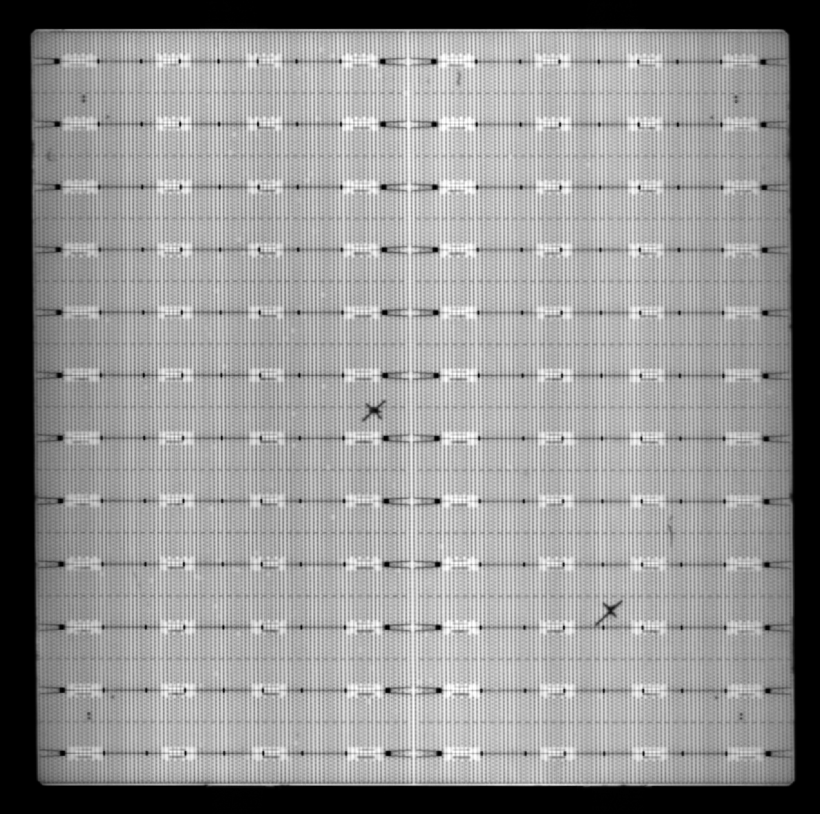
The production process of photovoltaic solar cells includes steps such as raw silicon wafer loading, cleaning, texturing, and etching. The initial raw silicon wafers are mostly provided by silicon material factories. Although these factories have strict control over product quality, batch issues, concentric circles, hidden cracks, and other defects may still occur. Additionally, transportation issues may lead to unavoidable defects such as hidden cracks, chipped edges, and contamination.

Based on the aforementioned defects, if they can be detected early, on one hand, they can be returned to the factory for replacement, and on the other hand, they can be removed before entering the next automated process, reducing the costs of manual cleaning and waste of downstream materials caused by an increase in scrap rate, as well as the production of non-A grade wafers. This can significantly reduce cost expenditures for battery factories and improve the yield of solar cells.

Technology Program

WPL addresses the aforementioned issues that arise in the incoming materials and corresponding production processes of raw silicon wafers
Developed an innovative technology for detecting defects in raw silicon wafers and launched a new OSI Light Source Module
  • By utilizing near-infrared laser light source and leveraging the laser's strong directionality for silicon wafer penetration, simultaneous detection of internal and edge defects is achieved.
  • After matching with a high-definition line scanning camera, it can be used to detect defects such as hidden cracks, dirt, broken edge, and unfilled corner in the raw silicon wafer.
  • The OSI Light Source Module is currently being used by leading battery manufacturers nationwide, with a pass-through rate of over 98.7%.
  • Combined with mature algorithms from users, the accuracy can reach over 97%. It has become a standard testing unit for today's PERC, TOPCon, and HJT.

Recommended Series

Recommended Model

Application Display

Industry Pain Points

Due to the lack of velvet-like light-trapping structures, the original silicon wafer differs significantly from the finished solar cell. The low light absorption efficiency of the original silicon wafer results in extremely low photoluminescence efficiency, making it extremely difficult to detect internal defects such as concentric circles and non-uniform silicon material that are not visible to the naked eye.

If the above-mentioned defects are not detected in a timely manner during the loading process, they may only be discovered during the final module manufacturing process, specifically during the Electroluminescence (EL) inspection stage. This results in low light emission efficiency of the solar cell, leading to its classification as B or C grade. Frequent occurrences of such situations can cause significant economic losses for battery and module manufacturing companies. Therefore, internal inspection of the original silicon wafer during the loading process becomes particularly important.

Technology Program

In response to the problem of extremely low photoluminescence efficiency of original silicon wafers, WPL has independently developed an integrated PL imaging module
The PL images of the original silicon battery cells can be transmitted to the PC through a gigabit network, and defects can be judged and eliminated through automation.
  • By applying optical technology to achieve a laser linewidth of 0.6mm, combined with a high sensitivity indium gallium arsenic camera, customers can easily achieve PL inspection of raw silicon wafers
  • The original silicon wafer PL detection scheme of WPL is often used for the detection of broken edge, unfilled corner, hidden cracks, and concentric circle defects after non-destructive scribing in heterojunction processes.

Recommended Series

Recommended Model

Application Display

Industry Pain Points

Due to various limitations, the current PERC, TOPCon, and HJT production lines are rarely able to achieve a full line layout and design from start to finish.

Coating loading is often carried out using VGA robots to connect with the carrier baskets. During the loading and gripping processes, there is a certain probability of causing hidden cracks, broken edges, or unfilled corners on the solar cells. Additionally, if there are process defects in the chemical cleaning stage, it can lead to issues such as uneven film deposition, black spots, and black cores after coating.

Technology Program

In order to avoid the above problems and waste of a large amount of materials in batch production. WPL launches PL detection solution after coating
By utilizing photoluminescence technology, it is possible to detect internal defects of each individual solar cell in real-time and at high speed. The proposed solution involves irradiating the solar cells with high-power near-infrared lasers that have a high absorption peak in silicon materials.
At the same time, choose an industrial grade camera with high sensitivity near-infrared light for internal image capture. Provide more effective reference analysis tools for on-site personnel to avoid the occurrence of batch defective films
  • Realize non-contact, high reliability, high stability, and high-speed online detection
  • The line laser is precisely aligned and calibrated with a line scan industrial camera, making it highly compatible with on-site installation requirements. It also facilitates easy repair and replacement if needed
  • The module is equipped with wired trigger and frame trigger functions to match different beats
  • A delay function has been developed to avoid issues such as image size being too large due to different sensor positions.

Recommended Series

Recommended Model

Application Display