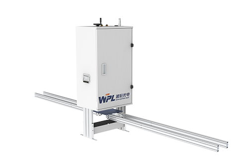
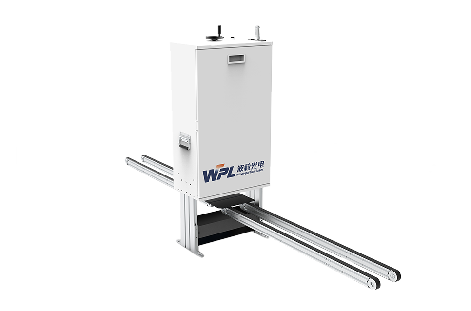
The LEP (Low Efficiency Photoluminescence) of modules are integrated PL imaging components specially developed for the low excitation efficiency of raw silicon wafers. They can transmit the PL images of raw silicon wafers to the PC through a gigabit network. Users can use image recognition related technologies to judge and identify defects in the imaging, and cooperate with automation to eliminate them.
Typical types of defects that can be detected are: hidden crack, broken edge, black center, concentric circle, scratch, belt mark and dirty.